Film Growth Laboratory
How do researchers grow thin films?
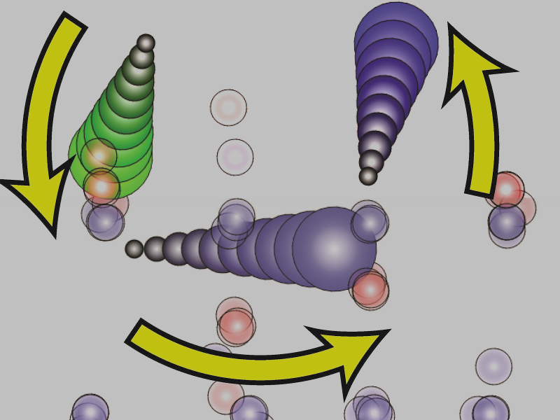
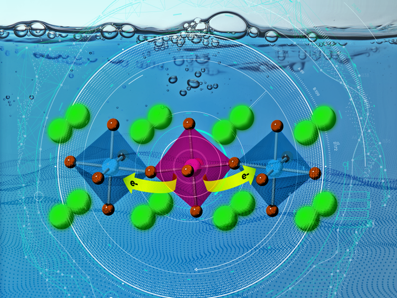
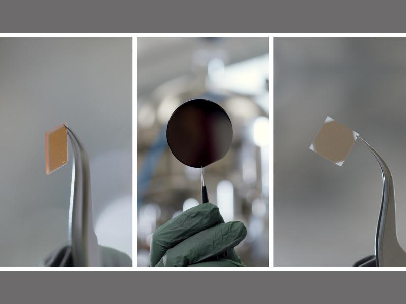
Thin films are an essential component of many modern electronics and are important for future energy applications. Being able to precisely grow thin films requires specialized equipment that enables researchers to add atoms to a surface layer by layer. The structure and composition of the resulting films can be tailored to study the fundamental properties of materials.
What is inside the Energy Sciences Center film growth laboratory?
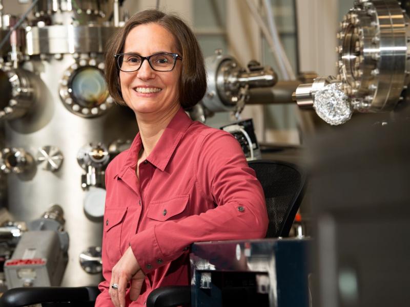
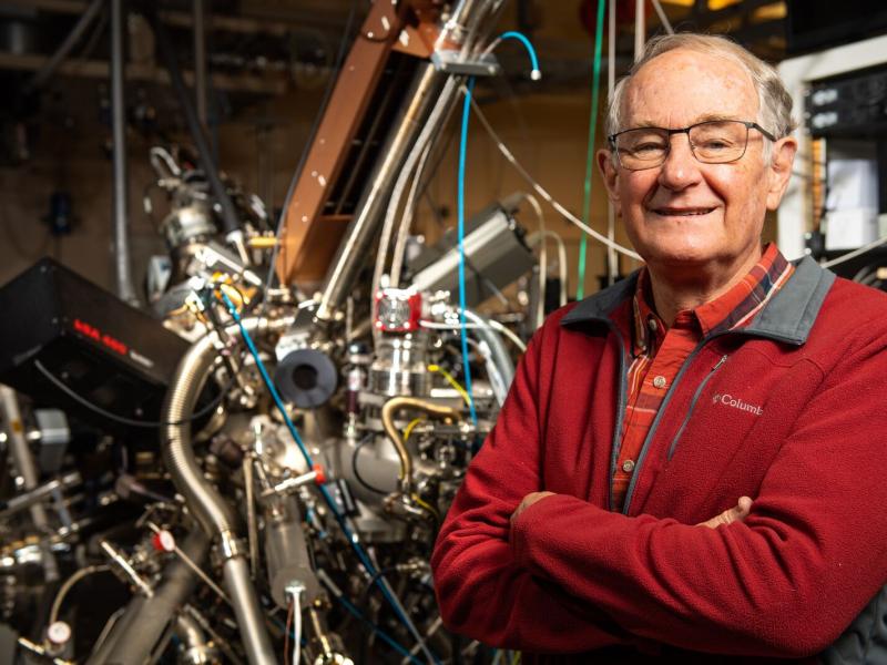
The film growth laboratory in the Energy Sciences Center (ESC) features two molecular beam epitaxy (MBE) and two pulsed laser deposition (PLD) systems. These instruments allow Pacific Northwest National Laboratory (PNNL) researchers to produce exceptionally high-quality thin films with precise control over a range of film properties while monitoring film growth.
The ESC’s two MBE systems use heat to vaporize up to 10 different elements at a time. This enables the PNNL researchers to create highly compositionally complex materials. The systems have in situ high-resolution X-ray photoelectron spectroscopy to characterize the created films without exposure to the air. This allows PNNL researchers to minimize any potential contamination of the precisely developed films.
The PLD systems hit high purity ceramic sources with a high-powered laser to eject the source material towards a surface. The (oftentimes complex) chemical composition of the source is maintained in the deposited thin film, but the film’s crystal structure is determined by the surface it is deposited on. The deposition process is controlled by computers, so the researchers can target and deposit multiple different ceramics in a specific sequence. This level of control enables the creation of complex structures, including films with elemental gradients and multiple layers.
