Precision
Materials
by Design
Precision
Materials
by Design
New nuclear and materials science capabilities in the Radiochemical Processing Laboratory (RPL) Radiological Microscopy Suite will benefit research across a number of disciplines. Researchers Edgar Buck (left) and Steven Spurgeon are among those using the 300kV JEOL GrandARM-300F aberration-corrected scanning transmission electron microscope.
(Photo by Andrea Starr | Pacific Northwest National Laboratory)
At PNNL, we use a combination of theory, computation, and experiments to advance knowledge-driven synthesis of materials for applications in energy, optics, electronics, and quantum information sciences.
Quantum materials synthesis and characterization
Much remains to be learned about the role of material purity in the function of quantum computing devices, starting with synthesis and continuing through to device fabrication. Improvements in quantum gate stability will depend in part upon precision materials characterization that relates structure (angstrom to micron scale) and purity (impurity analysis at the parts per trillion to parts per million scale) to device performance. To this end, PNNL combines expertise in controlled materials synthesis and precision characterization techniques, including:
- ultrathin crystalline nanosheets with well-defined molecular qubits
- thin film growth by molecular beam epitaxy and pulsed laser deposition
- aberration-corrected scanning transmission electron microscopy
- helium/neon ion microscopy/lithography
- plasma-based focused ion beam
- nano-/micro-computed tomography
- atom probe tomography
- large geometry secondary ion mass spectrometry
- multi-collector inductive-coupled plasma mass spectrometry.
Understanding atomic-to-mesoscale synthesis
To control the creation of new functional materials, it is crucial to understand the forces that act on them at different scales. Our studies range from subatomic to atomic, molecular, and nanoscale levels, and beyond. These fundamental studies lay the groundwork that will allow us to achieve real-time adaptive control over materials synthesis.
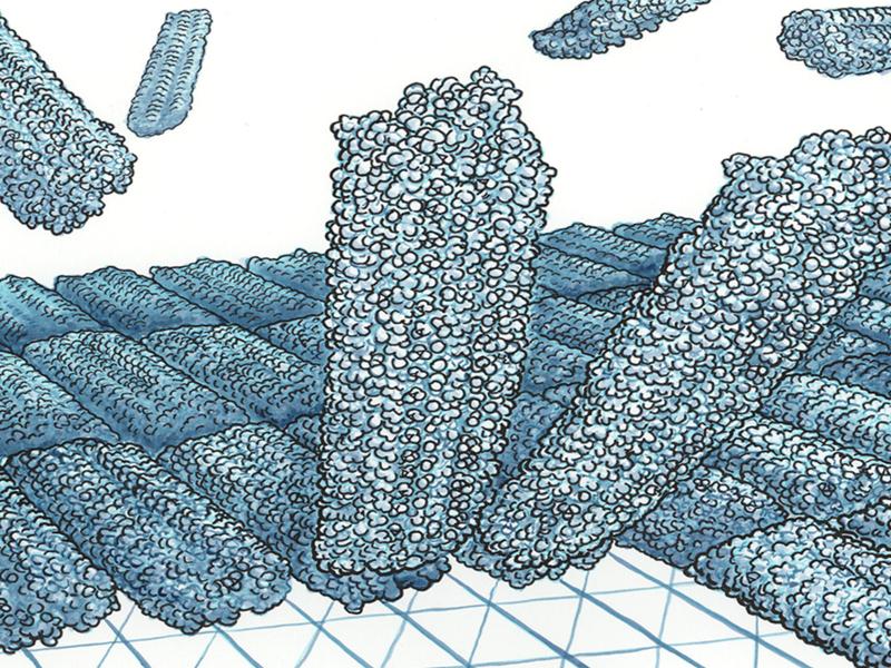
For instance, comprehending how superlattice structures form during nanoparticle self-assembly is important to tailoring their properties. However, key questions remain about how individual nanoparticles behave within emerging superlattice patterns. Researchers at PNNL are using advanced transmission electron microscopy equipped with direct detection camera capabilities to track individual nanoparticles in real time. From these measurements, they can calculate the atomic forces competing to drive the assembly process, providing a fundamental understanding of the dynamics involved in the assembly process, and ultimately enabling investigators to control the design of nanoparticle superlattices.
Unlocking new possibilities in atomically precise, layered materials
Through epitaxial growth techniques, including molecular beam epitaxy and pulsed laser deposition, researchers at PNNL can create precise stacks of multiple materials. Depending on the structure of the layers, the stacks can form into a superlattice that exhibits new properties. One such superlattice showed something unusual: electrons moved between different metal atoms where the layers met. By carefully measuring this charge flow and changing the thickness of the iron layer, scientists at PNNL discovered they could adjust the material’s electronic properties—like controlling how easily it conducts electricity. This finding is important because it shows that layering different materials can unlock new behaviors not seen in the individual materials. By fine-tuning how electrons move between layers, scientists can design advanced materials with specialized functions for next-generation electronics and energy storage technologies.
Designing polymers for complex structures
In nature, precise multi-component structures are found in materials ranging from bones to coral. Researchers at PNNL are using peptoids, human-designed peptide analogs, to develop materials with properties for applications ranging from drug delivery to microelectronics. The extensive tunability of the peptoids can produce a range of 2-D and 3-D structures, both individually and in combination with other materials. These materials are a centerpiece of biomimetic and bioinspired synthesis efforts at PNNL.

