High-Temperature Electrical Characterization Capability for Functional Materials
As a synergetic effort for synthesis and development of complex oxide and nanosheet materials, over the years, PNNL has developed electrical property characterization capabilities at temperatures from a few kelvins to room temperature.
Recently, PNNL has expanded this capability to include high temperatures up to 1200°C in a vacuum and a versatile electrical testbed to accommodate electrical property measurements of complex oxide and nanosheet materials. This testing infrastructure emulates the operation conditions of memristor devices in real-life applications and facilitates the fast characterization of electrical properties of novel functional materials as they are developed.
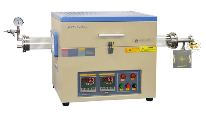
A key component of this setup is a two-zone tube furnace (MTI Corporation, model OTF-1200X-II-80) in conjunction with a turbo vacuum pumping system and gas flow control, providing variable testing environments to meet the requirements of different materials. A reliable and repeatable testing environment is achieved through digitalized process controls. Temperatures from the room temperature to 1200°C and vacuum from 10-6 torr to the atmospheric pressure are monitored and controlled using a computer program. Reactive and inert gases such as oxygen and nitrogen are purged in the tube furnace during different phases of the characterization via a computerized mass flow controller.
Another key component is an electrical circuit platform allowing electrical conductivity from the functional materials, which usually have features of interest in the sizes of nanometers to micrometers on substrates of a few millimeters in width to the macroscopic power sources and meters. This circuit board is customized on alumina to sustain high-temperature operations. Functional materials are wire bonded using gold wires of 25 micrometers in diameter to the circuit board which is connected to the external instruments through the vacuum feedthroughs. This setup allows up to 84 contacts wire bonded to functional materials at the same time and characterization of up to 32 pairs of contacts without breaking the vacuum.
The samples under test are usually micro-structures fabricated on complex oxide materials or their heterostructures using methods including thin film deposition, photolithography, and reactive ion etching. Four hall bar structures are fabricated on a 5mm by 5mm substrate and 36 electrical contacts are wire bonded to the alumina circuit board to measure the in-plane resistivity anisotropy. The electrical properties of 2D nanosheet materials may be characterized using the same method after patterned and transferred to the alumina circuit board.
The development of high-temperature electrical characterization for microfabricated materials provides fast feedback and optimization to the material synthesis processes and enables the rapid development of novel functional materials for many applications, including quantum computing.