August 1, 2022
Research Highlight

The Surprising Effect of Buried Homojunctions

Buried interfaces between sections of a doped material can play a key role in the overall electronic properties of the system

Generated image of a crystal structure

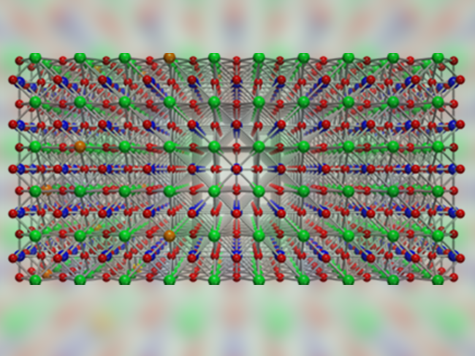
Research sheds considerable light on how trapped charge is partitioned between the surface and the buried interface in a complex layered oxide.

(Image by Scott Chambers | Pacific Northwest National Laboratory)

The Science                                

Semiconductor interfaces are critical for modern technology. Their properties can influence the behavior of the materials they connect, enhancing or diminishing performance in functional devices. Strontium titanium oxide (SrTiO3 or STO) is an oxide semiconductor with extremely high electron mobility but an unexplainably low dielectric constant. Whether STO is metallic or insulating depends on the presence (or absence) of electron-donating additive elements, known as dopants. New research identified that the interface between pure STO and STO with a very small percentage of the strontium atoms replaced by a dopant has a major impact on the resulting electrical properties of the overall material.

The Impact

Designing and fabricating semiconductor devices is a complex process. This process introduces interfaces that can affect the properties of the active layers. This work provides key insights into how device structure affects the measured oxide semiconductor properties and how engineering to create advanced structures can, in fact, mask the original useful properties of the material. These results have significantly deepened scientific understanding of the electronic properties of STO. They pave the way for fuller utilization of the desirable properties of complex oxide semiconductors in electronic devices.

Summary

Researchers prepared well-characterized capacitor and thin-film conductor structures entirely out of STO, a prototypical oxide semiconductor. They prepared layered structures of STO with and without low (≤ 1 atom %) concentrations of the electron-donating dopants dysprosium, lanthanum, niobium, and neodymium. The goal was to address two outstanding unsolved mysteries in the electronic properties of STO. These are: (1) why crystalline films of undoped STO have such low dielectric constants compared to bulk single crystals, and (2) why doped STO films always exhibit the apparent presence of electronically dead layers within the films despite their overall high conductivities.

To solve the first puzzle, researchers prepared an n-STO/undoped STO/n-STO structure with very few defects. n-STO refers to electron doped, where n stands for the negative charges in the STO. The two n-STO layers act as metal contacts for the capacitor. As expected, the overall measured capacitances were found to be substantially lower than that of bulk STO crystals. The researchers hypothesized that the two n-STO/STO interfaces had very low capacitances compared to the bulk of the undoped STO film between them. Modeling the system as three capacitors in a seriesone at each buried interface and one in the undoped filmshowed that the interface capacitances are exceedingly low. Once the contributions from the two buried interfaces were removed, the intrinsic dielectric constant of the high-quality undoped STO layer was revealed and found to be greater than that of the best STO single crystals measured to date.

The second puzzle was addressed by carefully probing conductive layer structures of an n-STO/undoped STO(001) structure to look for structural anomalies that might trap charge in the n-STO, giving rise to nonconductive layers within the overall conductive film. Soft X-ray photoemission did not show insulating layer formation near the surface. X-ray diffraction found evidence of lattice polarization, but modeling revealed that the polarized lattice would not trap charge. In contrast, analysis from modeling and hard X-ray photoemission that probes deeper into the sample revealed that both the buried interface and the surface can trap charge. However, the effects are sufficiently subtle to evade detection, even with state-of-the-art measurements. The amount of trapped charge detected using this analysis method for different n-STO film thicknesses quantitatively accounts for the measured dead-layer thicknesses determined by resistivity and Hall effect measurements.

PNNL Contact

Scott Chambers, Pacific Northwest National Laboratory, sa.chambers@pnnl.gov

Funding

Chambers et al. - Work at PNNL was supported by DOE, Office of Science, Division of Materials Sciences and Engineering. The team acknowledges support from the Oregon State University–PNNL Graduate Fellowship. Work at the University of Minnesota (UMN) was supported by DOE. Structural characterizations were carried out at the UMN Characterization Facility, which receives partial support from the National Science Foundation (NSF) through the MRSEC program. The team acknowledges support from the Air Force Office of Scientific Research and the Fine Theoretical Physics Institute of UMN. The modeling was done using the National Energy Research Scientific Computing Center, a DOE Office of Science user facility supported by the DOE Office of Science. This research used resources at the Advanced Photon Source, a DOE Office of Science user facility operated by Argonne National Laboratory.

Yang et al. - This work was primarily supported by the Air Force Office of Scientific Research. This work is also partially supported by the Vannevar Bush Faculty Fellowship and NSF through the Materials Research Science and Engineering Centers (MRSEC) program. Parts of this work were carried out at the Characterization Facility, University of Minnesota, which receives partial support from NSF through the MRSEC program. Device fabrication was carried out at the Minnesota Nano Center, which is supported by the NSF through the National Nano Coordinated Infrastructure. The work at Pacific Northwest National Laboratory (PNNL) was supported by the Department of Energy (DOE), Office of Science, Division of Materials Sciences and Engineering.

Published: August 1, 2022

S.A. Chambers, D. Lee, Z. Yang, Y. Huang, W. Samarakoon, H. Zhou, P.V. Sushko, T.K. Truttmann, L.W. Wangoh, T-.L. Lee, J. Gabel, and B. Jalan. “Combining in situ and ex situ Measurements to Probe Electronic Dead Layers in Homoepitaxial n-SrTiO3(001) Films,” APL Mater., 10, 070903 (2022). [DOI: 10.1063/5.0098500]

Z. Yang, D. Lee, J. Yue, J. Gabel, T.-L. Lee, R. D. James,S. Chambers, B. Jalan. “Epitaxial SrTiO3 Films with Dielectric Constants Exceeding 25,000,” Proc. Nat. Acad. Sci., 119, e2202189119 (2022). [DOI: 10.1073/pnas.2202189119].