3430 Clean Microfabrication Laboratory
Closing the gap between material development and application
United States
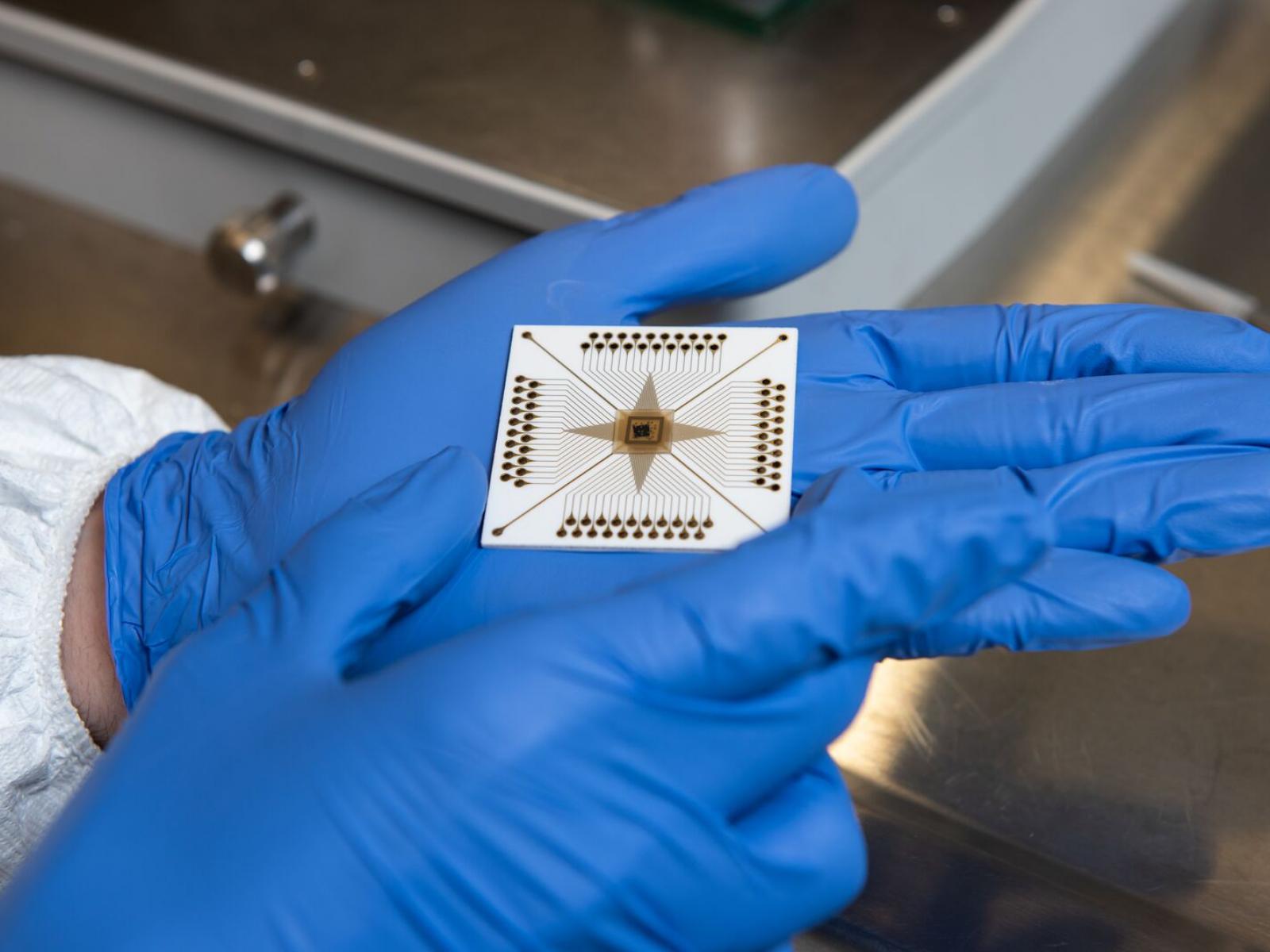
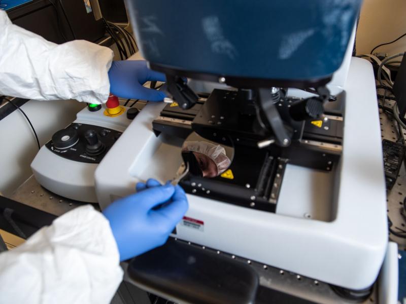
Complex oxide materials microfabricated in a hall bar pattern are wired bonded to a gold plated integrated circuit in PNNL’s clean microfabrication laboratory. The assembly will be measured to characterize the material transport properties in an electrical testbed developed at PNNL.
In the race to achieve quantum computing and quantum sensing, both high-energy physicists and computational scientists need advanced materials that can support their aims at the atomic level. A new clean microfabrication laboratory developed as part of PNNL’ s Chemical Dynamics Initiative creates a critical bridge between PNNL’s advanced material development and quantum applications, speeding work toward better understanding of materials and more efficient device manufacturing.
Microfabrication, the painstaking process of forming quantum devices, can only be carried out in dedicated cleanrooms. The new laboratory’s class 10,000 cleanroom is situated in the clean zone of Building 3430, a national security-approved, purpose-built facility designed with strict particle control measures including ceiling high-efficiency particulate air (HEPA) filters and entry protocols. These cleanroom conditions prevent small particles and disruptions that could otherwise destroy a microfabricated device.
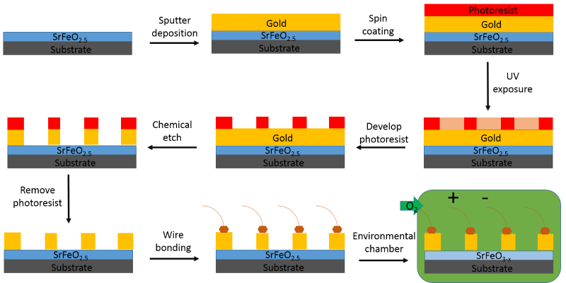
The laboratory streamlines the processes it conducts to build microfabricated devices using a full suite of technology in a single location. Co-located capabilities including thin film deposition, lithography, chemical etching, and wire bonding will replace current distributed production across smaller, widespread microfabrication laboratories. With the dedicated laboratory, researchers will be able to more quickly explore device architectures and build on PNNL’s strengths in synthesizing and characterizing complex materials to refine a material’s design with an eye toward its end use. The laboratory is scheduled for completion in summer 2021.
Instruments include the following:
- Magnetron sputtering system
- important all-around research tool in semiconductor, optics, solid-state research, and nanotechnology, the coating system uses magnetron sputtering as a source of deposition. The system is equipped with a 600 W DC and a 300 W 13.56 MHz RF gun for magnetic or non-magnetic metals and dielectric thin film depositions. The deposition vacuum system employs a 80 L/s turbo molecular pump and a full-range vacuum gauge to deliver vacuum from 760 Torr to 10-8 Torr. More than 20 deposition targets are available to provide essential thin films such as gold, aluminum, ITO, silicon oxide, etc.
- Reactive ion etch (RIE) system
- fully automated RIE system provides plasma etch capability on single wafers, dies, or parts using fluorine-, chlorine-, and oxygen-based chemistries. The system is equipped with a 600 W automatic tuning RF generator and chemical-resistant loadlock, gas chamber, and turbo pump. Highly selective anisotropic etching can be achieved on various materials such as Si, SiO2, SiN, GaAs, polyimide, and common metals.
- Wet chemical bench
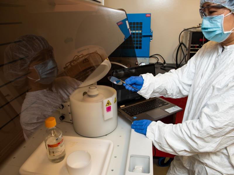
The chemical bench with a chemical-resistant high-density polypropylene working surface is used to carry out a wide range of processes involving chemicals such as solvents and acids. Chemical etching protocols including those for hydrofluoric acid have been developed to be used on this chemical bench. The bench is connected to de-ionized water, exhaust ventilation, and a drainage reservoir.
- Spin coater
Featuring a large range of speeds up to 12,000 rpm, the spin coater is used to achieve thin films, which are micron and sub-micron thick, using solutions of various viscosities. A typical application involves dispensing a photoresist solution on a wafer mounted in the center of the spin coater via vacuum. A multi-step spinning process removes excess solution and leaves a uniform thin film of the desired thickness.
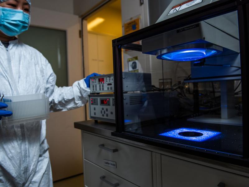
- NUV illumination system for photolithography
The near-ultraviolet (NUV) illumination system (350–450nm) provides a collimated wide area UV beam through which a pattern of micron to sub-micron resolution can be transferred to a photoresist. When a photoresist is exposed to this range of wavelength it undergoes a change in solubility with respect to a photoresist developer. The photoresist developing process and subsequent chemical etching are then carried out on the wet chemical bench until the pattern is transferred to the thin film underneath the photoresist.
- White light interferometry
The Bruker GT-I optical profilometer uses white light interferometry to characterize surface profiles in three dimensions. The system provides a nanometer resolution on measurements of thin film surface topography and roughness.
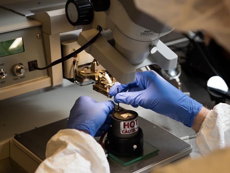
- Wire bonder
The wire bonder with a microscope viewer bonds gold or aluminum wires of micron sizes on microchips using ultrasonic energy. The conductive wires provide electricity from an external circuit to a microchip or between different parts of the microchip.
- Vacuum oven
The vacuum oven has a temperature range of room temperature to 230oC and operates under vacuum to zero Torr.
- Plasma cleaner
The plasma cleaner employs Ar or O2 plasma to clean organic contaminates from the substrate surfaces.