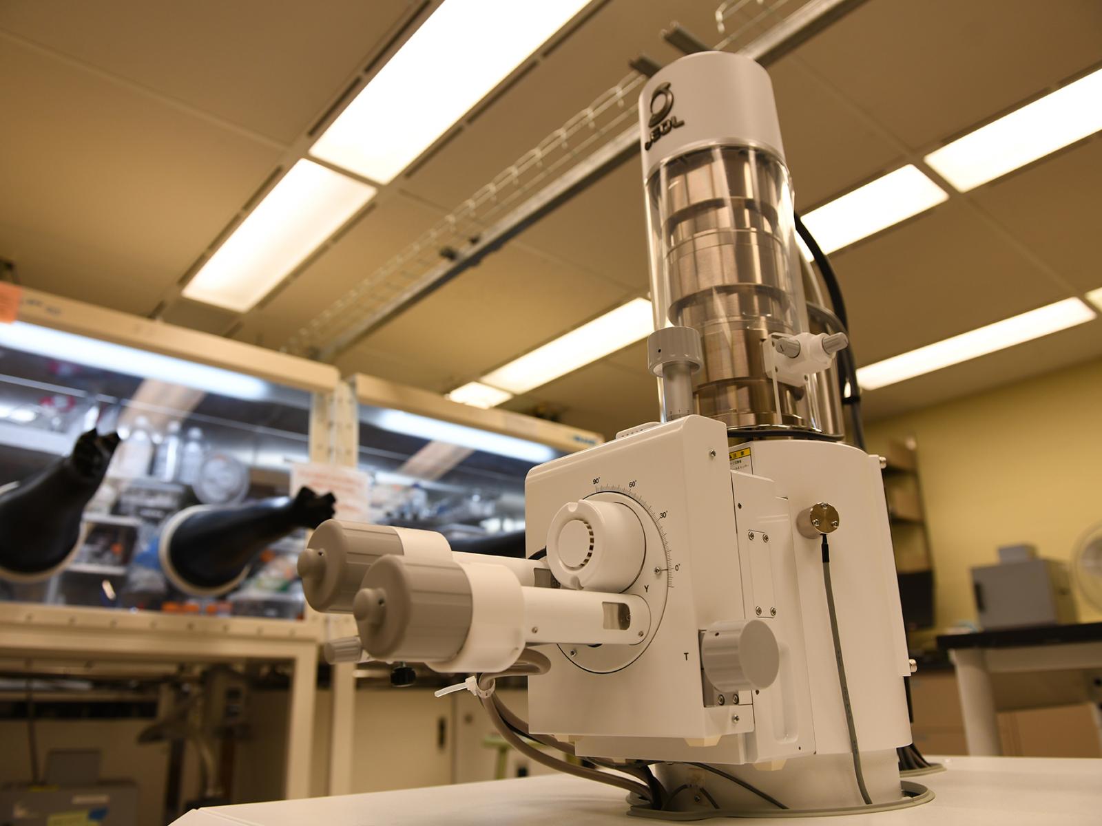
JEOL JSM-IT200LA Scanning Electron Microscope
Located in PSL | Stewarded by Jiangtao Hu and Lorraine Seymour, Battery Materials & Systems Group
Andrea Starr | Pacific Northwest National Laboratory
Located in PSL | Stewarded by Jiangtao Hu and Lorraine Seymour, Battery Materials & Systems Group
Andrea Starr | Pacific Northwest National Laboratory
Mission
The JEOL JSM-IT200LA Scanning Electron Microscope (SEM) provides high-resolution and high-throughput microstructural characterization support to PNNL’s battery materials science research. This instrument can be used on non-dispersible materials with permission from the instrument stewards.
Features